Chasing an RFI Problem: Home-Automation Touch Panels and My CW Signal
30/08/2026
This is a write-up of a measurement campaign, not a story with a happy ending. I still don't have a clean fix. What I do have is a fairly complete picture of how a low-power amateur signal ends up switching a capacitive glass touch panel, backed by numbers from a controlled test setup. This post is just the measurements and the technical conclusions that follow from them.
The symptom
I run QRP. During telegraphy experiments on the 40 m band at 5 W, capacitive glass touch panels in my home-automation installation switched on their own at the moment of transmission. With a constant, unmodulated carrier the panels were not just twitchy but unresponsive — and they stayed unusable for a while after the RF was gone.
The fault is not consistent. In unattended WSPR runs a false trigger sometimes took several days to show up. It is also not confined to my own house: panels next door have been switched by my transmissions, and at 50 W (borrowed radio, for testing) modules two houses away reacted.
Two early clues framed everything that followed:
- The problem is overwhelmingly a 40 m phenomenon. Higher HF bands are affected but less so; VHF/UHF only at very short range.
- A more recently produced panel with a fully closed plastic back showed no interference at all under the same conditions, with a magnetic loop held right next to it.
Because my antenna is an end-fed half-wave — inherently asymmetric — common-mode current on the coax shield was the obvious first suspect. I built a common-mode choke with ~40 dB of attenuation and put it in the feedline. Big improvement, not a cure. That pointed at direct field coupling into the installation, and that is where the real investigation started.
First investigations
Frequency dependence
Transmitting indoors with a 1 m magnetic loop (re-tuned per frequency), held a few centimetres from a panel, the switches misfired at absurdly low power. Later, once I had a field-strength meter, I could put a number on that specific test: it corresponded to roughly 70 V/m at the panel, so it is not conclusive on its own — but the frequency profile is telling.
| Frequency | Observation |
|---|---|
| 3.8 MHz | no interference at 5 W |
| 7.0 MHz | interference at ~10 mW (loop at 5 cm) |
| 7–28 MHz | interference across the band, somewhat less sensitive |
| 145 MHz | interference only at a few cm, at 5 W |
| 435 MHz | interference at 0.5 W at 1 cm |
The conducted path via the bus cable
At these frequencies I initially assumed the energy had to be arriving on the bus cable — radiated-emission testing in an EMC lab only starts at 80 MHz, and the bus wiring in the house is plausibly a multiple of a half wavelength on 40 m. I wound 10 turns of bus cable on an Amidon FT-140-31 ferrite core and measured 29.18 dB of common-mode attenuation at 7 MHz on a nanoVNA.
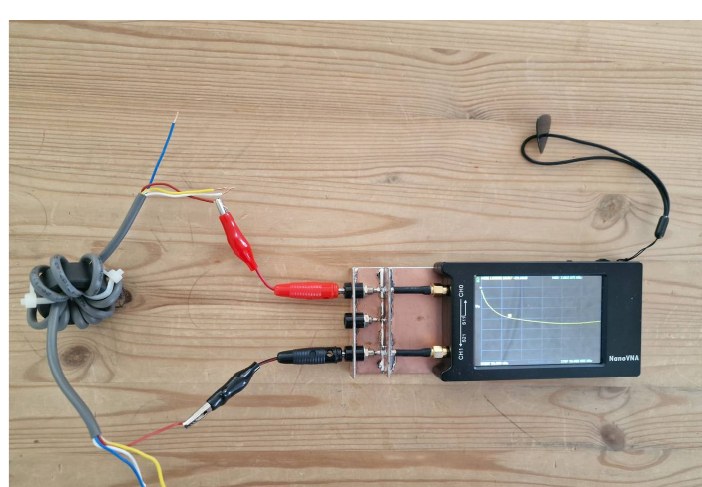
This choke went in at several points in the installation, including on both the primary and secondary side of the supply. The last module in the chain was consistently the most sensitive — exactly what you'd expect if the wiring behaves like an antenna and the far end carries the highest voltage. A ferrite on the second-to-last module produced a noticeable improvement. I never managed to solve it structurally across the whole house.
The radiated path
So I went back to direct field coupling. I disconnected one module completely and powered it from a 12 V battery on ~10 cm leads — no bus, no mains, no earth.
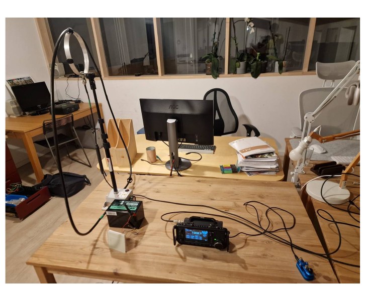
Same fault, same low power. As with the earlier test, the field at the module was later estimated at ~70 V/m, so the absolute number is soft — but it proves that direct field coupling onto the electrode is a sufficient path on its own, with nothing else connected.
Field strength
With a borrowed field-strength meter (isotropic-ish probe, no polarisation discrimination), I started with a 10 W unmodulated carrier on 7 MHz into the EFHW. The highest reading was at the last module in the bus chain: 13.7 V/m, and that module was unresponsive at the time.
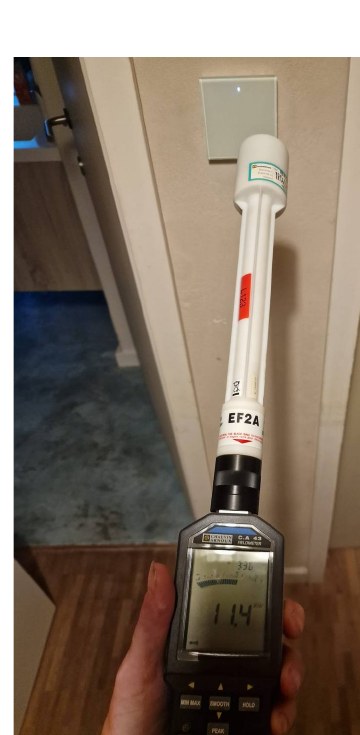
Two things stood out:
- The bus cable re-radiates. Where I measured 13.7 V/m right next to the switch, the middle of the same room read only 4–6 V/m.
- Measurements near a switch or antenna are extremely position-sensitive. A few centimetres of probe movement changed the reading substantially.
A useful control observation: the house on the other side is also fitted with the same automation system, but with in-wall modules behind mechanical pushbuttons instead of glass touch panels. It has never shown any interference.
Why capacitive touch is vulnerable here
A bit of background reading showed this is well documented in the amateur world — the ARRL keeps a page on RFI to touch lamps, with cases fixed by a series resistor in the sensing line or an RF choke. The same behaviour has been reported by others on these panels too, in one case triggered not by RF at all but by mains disturbance from a solar inverter — and again only the older modules were affected.
Opening a switch explains a lot:
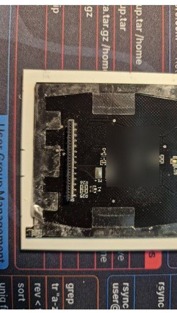
- The electrode board is glued to the glass and connects to the controller board through a pin header.
- The electrodes go straight into analog inputs of the microcontroller. There is no series impedance anywhere in that path — no resistor, no ferrite bead, no filter.
- The back of the electrode board carries a hatched copper pour. That limits parasitic capacitance and crosstalk, but does nothing to suppress RF ingress.
- The board has four separately-read electrode zones. On the single-channel version, touching any of the four does the same thing — presumably one board design serves the 1-, 2- and 4-channel products. For immunity that isn't free: a single-channel panel is then four independent detectors in effective OR, over four times the collecting area it functionally needs — statistically ~6 dB more sensitive than one channel.
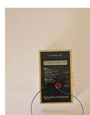
A finger through the glass is a change of 1.3–1.6 pF. With a charging current of a few microamps for a few microseconds, on a node of a few tens of pF, that works out to a few tens of mV at the analog input.
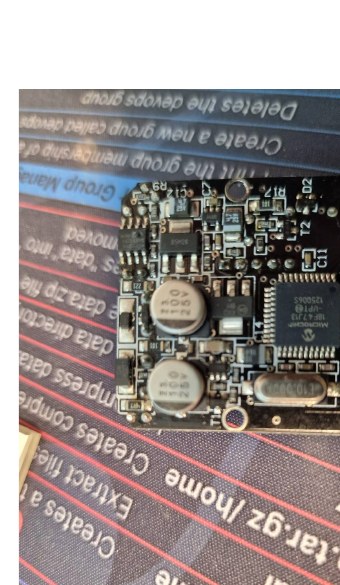
The controller is a Microchip PIC18F47J13. There is no separate touch controller — capacitive sensing is done in the MCU itself, which points to the CTMU (Charge Time Measurement Unit) method.
Putting it together:
- Induced voltage on a small electrode is roughly V = E × h_eff. For a few-cm electrode in a 10 V/m field that's on the order of 150 mV of RF, essentially frequency-independent.
- What normally makes a tiny electrode useless as an antenna is its high source impedance. But a microcontroller analog input is itself almost infinitely high-impedance, so there's no voltage division and the full induced voltage sits on the pin — the same principle as a Mini-Whip receive antenna.
- The CTMU charges the sensor with a constant current for a fixed time; the ADC reads the resulting voltage, inversely proportional to capacitance. Incoming RF gets rectified in the protection diodes and the ADC sample-and-hold, producing a DC offset that is indistinguishable from a real touch.
- Why it's worst at the low end of HF: the electrode capacitance and the parasitic shunt capacitances scale together, so their ratio stays roughly flat. What changes is the behaviour after the pin — internal inductances become high-impedance with rising frequency and the rectification gets less efficient.
- There is a second, independent path via the supply conductors. The ADC conversion is typically ratiometric to the supply, and in a compact install there is no separate stable ground reference: moduleGND is itself the reference against which both the supply and the sensing are measured. RF arriving on the supply can therefore shift the ADC reference directly, or move the reference point relative to the electrode.
A controlled test setup
To get away from the position sensitivity and the erratic coupling of a hand-held probe, I built a parallel-plate jig: two PCB panels, 570 × 510 mm, 30 cm apart, fed at one end and terminated in 50 Ω at the other.
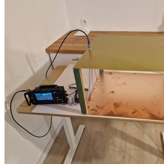
The principle is a TEM cell, except the impedance isn't matched and the field isn't contained — I have a permit for 40 m, so that's fine. At 7 MHz the wavelength is 43 m, so a jig this size stays electrically small and the field between the plates follows E = V/d with no correction terms. I validated it by placing the field-strength meter between the plates in various orientations; the reading matched the calculation. Unlike a hand-held measurement in the house, this gives a spatially uniform, position-independent field, so every threshold below is repeatable.
Two independent coupling paths, quantified
Sweeping the field until the switch reacted:
| Configuration | Threshold |
|---|---|
| Fully isolated module, battery, 10 cm lead | ~50 V/m |
| Module + ~10 m of bus cable to the battery | 11–15 V/m |
| Same, bus cable coiled up inside the jig | 7 V/m |
The 11–15 V/m figure matches what I'd measured in the house. Coupling is strongest with the panel upright and the E-field perpendicular to its face. The coiled-cable case is not a measurement error: the cable takes energy out of the ambient field and concentrates it locally at the module — a real re-radiation effect that every practical installation brings with it via its own wiring. (Strictly, coiling the cable is not compliant with EN IEC 61000-4-3, which calibrates the field in an empty room with the cable pulled straight; it just illustrates the mechanism well.)
Confirming a conducted path via the supply
To separate "the cable locally boosts the field" from "the cable delivers a conducted signal", I aimed the RF source at only the cable, with the module and its electrode out of the direct field. The module still switched.
Then I disconnected the data lines, leaving only the two supply conductors (+ and GND). No change. So the conducted path runs via the supply conductors, not the data lines. In this isolated setup, supply and sensing reference are the same node — the battery minus, which is also moduleGND and the reference for the capacitive sensing. RF current entering on that conductor shifts the measurement's reference point directly. That's the mechanism suspected from the start, now confirmed.
Measures tested
1 — Series resistors in the electrode lines
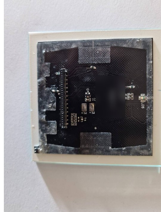
SMD resistors on the board itself and in the pin header (easy to fit), tried at 1 kΩ and 10 kΩ. They made things worse: a switch that reacted from 13 V/m before was down to 8 V/m after. Reverted.
2 — Common-mode choke on the bus line
Test setup: 10 m of bus cable coiled in the jig together with the switch. Baseline in that configuration was switching at 8 V/m at 7 MHz.
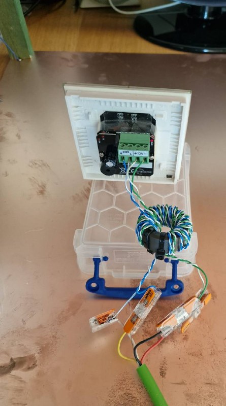
For high suppression on HF I used mix 31. An FT-140-31 is the largest core I can hide behind a switch. Using separate wires I got 15 turns on, just under 30 dB of suppression at 7 MHz on the nanoVNA, self-resonance well above 30 MHz. Result: the switch now fails at 13 V/m instead of 8. An improvement, but less than I'd hoped for from 30 dB.
3 — Shielding
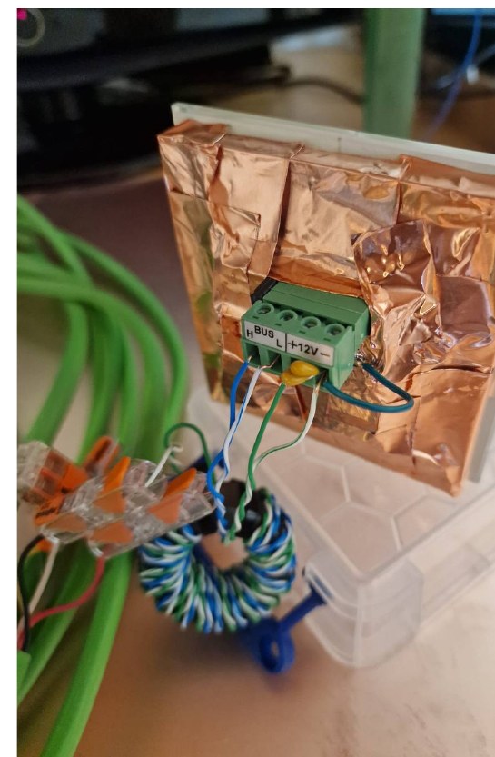
The back of the switch wrapped in copper foil, tied to moduleGND with a short wire. The first results were good: common-mode choke + shielding + supply decoupling (100 nF + 1 nF ceramic on AVDD/AVSS) pushed the threshold to 30 V/m.
But when I reshaped the foil so it could actually fit inside a standard flush-mount box, the result collapsed. Best I got in a box-compatible form was 16 V/m — an improvement, but too little to roll out across every switch.
Where that leaves it
The three supply-side measures together (choke, decoupling, grounding) raised the threshold to at most 30 V/m in the jig — measurable, but not a structural fix, and not practical once the shielding has to fit a standard flush box. Two explanations remain open, and neither is reachable with external components:
- Coupling inside the microcontroller itself, between the supply pins and the internal sensing reference.
- Crosstalk on the board or the connector, between the (necessarily connected) supply pins and the completely unprotected electrode traces right next to them on the same header — a path that has already done its work before any external filter.
By contrast with the series-resistor idea, these can't be fixed by bolting parts on the outside.
Instruments
| Instrument | Use |
|---|---|
| Icom IC-705 | QRP transceiver, ≤10 W on HF |
| Icom IC-7300 (borrowed) | higher-power tests, ≤100 W on HF |
| Chameleon CHA F-LOOP | 1 m magnetic loop, tunable, very high Q |
| nanoVNA-H4 | common-mode suppression measurements |
| Chauvin Arnoux C.A. 43 + EF2A probe | absolute field strength, house and jig |
| AADE LC Meter IIB (kit), 0.02 pF resolution | sensor-signal characterisation |
| Homebuilt parallel-plate jig (2× 570 × 510 mm PCB, 30 cm) | controlled, uniform E-field for threshold measurement |
Conclusions
- Direct field coupling onto the electrode is sufficient on its own. A fully isolated module on a battery, no bus, no mains, no earth, still misfires — at ~50 V/m in the controlled jig, and much lower with any wiring attached.
- The wiring dominates in practice. Attaching ~10 m of bus cable drops the threshold from ~50 V/m to 11–15 V/m, and the cable re-radiates the ambient field into a local hot-spot at the module. The far end of the bus chain is always the worst.
- There are two independent coupling paths. One radiated, onto the electrode; one conducted, via the supply conductors (not the data lines), shifting the sensing reference. Any fix has to address both.
- RF rectification in the input structure turns an induced ~150 mV of RF into a DC offset that the CTMU cannot distinguish from a finger. The absence of any series impedance in the electrode path, plus four OR'd detectors on the single-channel variant (~6 dB), plus a high-impedance node behaving like a Mini-Whip, all stack the odds against immunity at the low end of HF.
- External mitigation helps but doesn't cure. Best case with common-mode choke + supply decoupling + full copper-foil shielding was 30 V/m in the jig; in a form that fits a standard flush box, 16 V/m. Series resistors in the sensing lines made it worse.
- A series resistor between electrode and MCU pin — done at design time — is the one change from the standard robust-touch guidance (Microchip AN1334) that would actually help here, and it's the one thing that can't be retrofitted.
- For context on exposure: VLAREM II art. 2.14.2.1 gives a reference level of E = 150·f-0.7 V/m for 0.1–30 MHz, i.e. 38.4 V/m at 7 MHz as a 30-minute average. My measured pure-carrier maximum was ~15 V/m; with CW keying duty (~45% power) that's ~10 V/m as a 30-minute average. The interference sits right on the edge of perceptibility — sometimes several days pass with no false switching at all.
References
- ARRL, RFI — Touch Lamp & Lamp Dimmer — www.arrl.org/touch-lamp
- Microchip, PIC18F47J13 datasheet (CTMU)
- Microchip, AN1250 — CTMU for Capacitive Touch Applications
- Microchip, AN1334 — Techniques for Robust Touch Sensing Design
- EN IEC 61000-4-3, EN IEC 61000-4-6, EN IEC 61000-6-1
73, ON4DMD
Comments